Let’s be honest, when we talk about the AI boom, our minds usually jump to two things: mind-bending software like ChatGPT and the super-powerful chips from Nvidia that make it all possible. It’s the sexy, headline-grabbing stuff.
But what if I told you the most important battle for the future of AI isn't just about making chips faster? What if it's about how we connect them?
It sounds almost ridiculously boring, I know. The technology is called "advanced packaging," and on the surface, it sounds about as exciting as wrapping a birthday present. But this is where Intel is placing a multi-billion-dollar bet that could completely reshape the tech world. And frankly, it’s one of the most fascinating comeback stories brewing in Silicon Valley.
So, stick with me for a minute. Let's unpack this (pun absolutely intended) and figure out why this nerdy, under-the-radar tech has suddenly become the key to everything.
So, What on Earth is 'Advanced Chip Packaging'?
For decades, the name of the game in the chip world was Moore's Law. The simple goal was to cram more and more tiny transistors onto a single slice of silicon. Think of it like building a city by making every single brick smaller and smaller, allowing you to fit more buildings into the same plot of land.
That worked brilliantly for 50 years. But we're hitting a wall. We're now dealing with components so small that the laws of physics are starting to push back. Making the bricks smaller is getting insanely difficult and expensive.
This is where advanced packaging comes in.
Instead of just building a flat, sprawling city (a traditional circuit board), what if we started building up? What if we could stack different specialized chips on top of each other, like a skyscraper, and connect them with tiny, ultra-fast elevators?
That, in a nutshell, is advanced packaging. It's the art and science of taking multiple small chips, or "chiplets," and combining them into a single, powerful, three-dimensional package. One chiplet might handle processing, another might be for memory, and a third could manage graphics—all sitting together in a tightly integrated, high-performance unit.
It’s a shift from a 2D world to a 3D world, and it’s a total game-changer for performance.
Intel's Throwing Everything at This
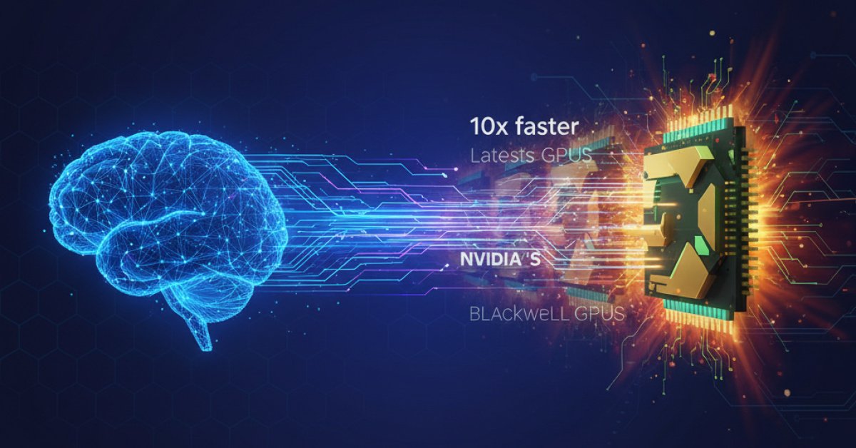
For years, Intel watched from the sidelines as Taiwan's TSMC became the world's go-to factory for high-end chips, especially for companies like Apple and Nvidia. TSMC perfected its own advanced packaging technology, and it's a huge reason why Nvidia's AI GPUs are so dominant.
Now, Intel is roaring back with a vengeance, and packaging is the heart of its strategy. They're not just dipping their toes in the water; they're cannonballing into the deep end.
Here’s the plan:
- They're opening their doors. In a huge shift, Intel is now acting as a "foundry," meaning they'll build chips for other companies. Yes, even their rivals. They want their cutting-edge packaging tech to be so good that everyone will want to use it.
- They're spending billions. We're talking massive new factories in Arizona, Ohio, and even Germany, all equipped with the machinery for this complex 3D stacking. This isn't a side hustle; it's the core of their future.
They have two key technologies they're banking on:
- Foveros: This is their 3D stacking tech. It's the "skyscraper" I was talking about. It allows them to stack logic chips on top of each other for a massive density and performance boost.
- EMIB (Embedded Multi-die Interconnect Bridge): This is more like a tiny, super-fast underground tunnel that connects different chiplets side-by-side on a 2D plane. It's for when you don't need a full skyscraper but still need an express connection between two buildings.
By combining these, Intel can basically build custom, high-performance systems for anyone, mixing and matching the best chiplets for the job. It's like building with the most advanced LEGOs in the world.
Why Does This Matter So Much for AI?
Okay, so we're stacking chips. Cool. Why is this suddenly the key to the AI kingdom?
It all comes down to one word: bottlenecks.
Think of a large language model like the ones that power AI chatbots. To work their magic, they need to move absolutely staggering amounts of data between the processor and the memory, and they need to do it almost instantly.
You can have the fastest processor core in the world, but if it's sitting there waiting for data to arrive, it's useless. It's like having a brilliant chef who can cook a five-course meal in ten minutes, but the ingredients are being delivered by a guy on a bicycle from across town. The chef is just going to be standing around, waiting.
Traditional chip design puts the processor and memory relatively far apart on a circuit board. The distance, as tiny as it seems to us, is a massive traffic jam at the speeds these components operate.
Advanced packaging solves this. By stacking the memory right on top of or right next to the processor, you shrink that distance down to almost nothing. You replace the bicycle with a direct, high-speed pneumatic tube. This is what's known as "high-bandwidth memory" (HBM), and it's absolutely essential for high-end AI.
The result? The chef gets their ingredients instantly. The AI model gets its data without delay. And you get faster, more powerful, and more efficient artificial intelligence.
A High-Stakes Game With a Massive Payoff
Now, let's be clear: this is a huge gamble for Intel.
This stuff is incredibly hard to do. We're talking about connecting microscopic layers of silicon with perfect precision. One tiny error, one misplaced connection, and the entire, expensive package is a dud. The manufacturing yields (the percentage of good chips vs. bad ones) have to be near-perfect to make it profitable.
And the competition isn't sleeping. TSMC is the established leader and is pushing its own technology forward. Samsung is also a major player pouring billions into its own packaging solutions.
But if Intel can pull this off? The reward is astronomical.
If they can prove their packaging is the best in the business, they won't just be making their own chips anymore. They could become the indispensable manufacturing partner for the entire AI industry. Companies designing the next generation of AI hardware would have to come to Intel to get it built.
It would be one of the most incredible comeback stories in tech history, cementing Intel's relevance for decades to come. It’s a bet that the "box" the chip comes in is just as important as the chip itself.
So next time you see a flashy AI demo, remember the unsung hero. The real magic isn't just in the code or the silicon brain. It's in the incredibly complex, three-dimensional city of chips working together in perfect harmony. And Intel is betting its entire future that it can become the master architect of that city. It's a nerdy bet, for sure, but it could be the one that pays off in billions.